System Design Considerations
- In optical system design major consideration involves
- Transmission characteristics of fiber (attenuation & dispersion).
- Information transfer capability of fiber.
- Terminal equipment &
- Distance of
- In long-haul communication applications repeaters are inserted at regular intervals as shown in Fig. 6.2.1

- Repeater regenerates the original data before it is retransmitted as a digital optical The cost of system and complexity increases because of installation of repeaters.
- An optical communication system should have following basic required specifications –
- Transmission type (Analog / digital).
- System fidelity (SNR / BER)
- Required transmission bandwidth
- Acceptable repeater spacing
- Cost of system
- Reliability
- Cost of maintenance
Multiplexing
- Multiplexing of several signals on a single fiber increases information transfer rate of communication In Time Division Multiplexing (TDM) pulses from multiple channels are interleaved and transmitted sequentially, it enhance the bandwidth utilization of a single fiber link.
- In Frequency Division Multiplexing (FDM) the optical channel bandwidth is divided inot various nonoverlapping frequency bands and each signal is assigned one of these bands of By suitable filtering the combined FDM signal can be retrieved.
- When number of optical sources operating at different wavelengths are to be sent on single fiber link Wavelength Division Multiplexing (WDM) is used. At receiver end, the separation or extraction of optical signal is performed by optical filters (interference filters, differaction filters prism filters).
- Another technique called Space Division Multiplexing (SDM) used separate fiber within fiber bundle for each signal SDM provides better optical isolation which eliminates cross-coupling between channels. But this technique requires huge number of optical components (fiber, connector, sources, detectors etc) therefore not widely used.
System Architecture
- From architecture point of view fiber optic communication can be classified into three major
- Point – to – point links
- Distributed networks
- Local area
Point-to-Point Links
- A point-to-point link comprises of one transmitter and a receiver system. This is the simplest form of optical communication link and it sets the basis for examining complex optical communication links.
- For analyzing the performance of any link following important aspects are to be
- Distance of transmission
- Channel data rate
- Bit-error rate
- All above parameters of transmission link are associated with the characteristics of various devices employed in the link. Important components and their characteristics are listed

- When the link length extends between 20 to 100 km, losses associated with fiber cable In order to compensate the losses optical amplifier and regenerators are used over the span of fiber cable. A regenerator is a receiver and transmitter pair which detects incoming optical signal, recovers the bit stream electrically and again convert back into optical from by modulating an optical source. An optical amplifier amplify the optical bit stream without converting it into electrical form.
- The spacing between two repeater or optical amplifier is called as repeater spacing (L). The repeater spacing L depends on bit rate B. The bit rate-distance product (BL) is a measure of system performance for point-to-point links.
- Two important analysis for deciding performance of any fiber link are –
- Link power budget / Power budget
- Rise time budget / Bandwidth budget
- The Link power budget analysis is used to determine whether the receiver has sufficient power to achieve the desired signal The power at receiver is the transmitted power minus link losses.
- The components in the link must be switched fast enough and the fiber dispersion must be low enough to meet the bandwidth requirements of the Adequate bandwidth for a system can be assured by developing a rise time budget.
System Consideration
- Before selecting suitable components, the operating wavelength for the system is The operating wavelength selection depends on the distance and attenuation. For shorter distance, the 800-900 nm region is preferred but for longer distance 100 or 1550 nm region is preferred due to lower attenuations and dispersion.
- The next step is selection of photodetector. While selecting a photodetector following factors are considered –
- Minimum optical power that must fall on photodetector to satisfy BER at specified data
- Complexity of
- Cost of
- Bias
- Next step in system consideration is choosing a proper optical source, important factors to consider are –
- Signal
- Data
- Transmission
- Optical power
- Circuit
- The last factor in system consideration is to selection of optical fiber between single mode and multimode fiber with step or graded index fiber. Fiber selection depends on type of optical source and tolerable dispersion. Some important factors for selection of fiber are :
- Numerical Aperture (NA), as NA increases, the fiber coupled power increases also the dispersion.
- Attenuation
- Environmental induced losses e.g. due to temperature variation, moisture and dust
Link Power Budget
- For optiming link power budget an optical power loss model is to be studied as shown in 6.2.3. Let lc denotes the losses occur at connector.
Lsp denotes the losses occur at splices. αf denotes the losses occur in fiber.
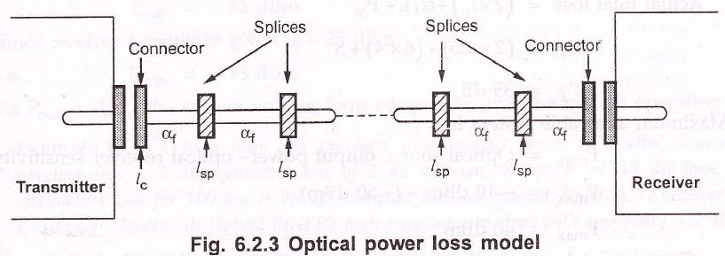
- All the losses from source to detector comprises the total loss (PT) in the
- Link power margin considers the losses due to component aging and temperature Usually a link margin of 6-8 dB is considered while estimating link power budget.
- Total optical loss = Connector loss + (Splicing loss + Fiber attenuation) + System margin (Pm)
PT = 2lc + αfL + System margin (Pm) where, L is transmission distance.
Example 6.2.1 : Design as optical fiber link for transmitting 15 Mb/sec of data for a distance of 4 km with BER of 10-9.
Solution :
Bandwidth x Length = 15 Mb/sec x 4 km = (60 Mb/sec) km
Selecting optical source : LED at 820 nm is suitable for short distances. The LED generates – 10 dBm optical power.
Selecting optical detector : PIN-FER optical detector is reliable and has – 50 dBm sensitivity.
Selection optical fiber : Step-index multimode fiber is selected. The fiber has bandwidth length product of 100 (Mb/s) km.
Links power budget :
Assuming :
Splicing loss ls = 0.5 dB/slice Connector loss lc = 1.5 dB
System link powr margin Pm – 8 dB Fiber attenuation αf = 6 dB/km Actual total loss = (2 x lc) + αfL + Pm
PT = (2 x 1.5) + (6 x 4) + 8 PT = 35 dB
Maximum allowable system loss :
Pmax = Optical source output power- optical receiver sensitivity Pmax = -10 dBm – (-50 dBm)
Pmax = 40 dBm
Since actual losses in the system are less than the allowable loss, hence the system is functional.
Example 6.2.2 : A transmitter has an output power of 0.1 mW. It is used with a fiber having NA
= 0.25, attenuation of 6 dB/km and length 0.5 km. The link contains two connectors of 2 dB average loss. The receiver has a minimum acceptable power (sensitivity) of – 35 dBm. The designer has allowed a 4 dB margin. Calculate the link power budget.
Solution :
Source power Ps = 0.1 mW
Ps = -10dBm
Since NA = 0.25
\ Coupling loss = -10log (NA2)
= -10log (0.252)
= 12 dB
Fiber loss = αf x L
lf = (6dB/km) (0.5km) lf = 3 dB
Connector loss = 2 (2 dB)
lc = 4 dB Design margin Pm = 4 dB
\ Actual output power Pout = Source power – (Σ Losses) Pout = 10dBm – [12 dB + 3 + 4 + 4]
Pout = -33 dBm
Since receiver sensitivity given is – 35 dBm.
- Pmin = -35 dBm
As Pout > Pmin, the system will perform adequately over the system operating life.
Example 6.2.3 : In a fiber link the laser diode output power is 5 dBm, source-fiber coupling loss
= 3 dB, connector loss of 2 dB and has 50 splices of 0.1 dB loss. Fiber attenuation loss for 100 km is 25 dB, compute the loss margin for i) APD receiver with sensitivity – 40 dBm ii) Hybrid PINFET high impedance receiver with sensitivity -32 dBm.
Solution : Power budget calculations
|
Source output power |
5 dBm |
|
Source fiber coupling loss |
3 dB |
|
Connector loss |
2 dB |
|
Connector loss |
5 dB |
|
Fiber attenuation |
25 dB |
Total loss 35 dB
Available power to receiver : (5 dBm – 35 dBm) – 30 dBm
- APD receiver sensitivity – 40 dBm
Loss margin [- 40 – (- 30)] 10dBm
- H-PIN FET high0impedance receiver -32 dBm Loss margin [- 32 – (- 30)] 2 dBm
Rise Time Budget
- Rise time gives important information for initial system design. Rise-time budget analysis determines the dispersion limitation of an optical fiber link.
- Total rise time of a fiber link is the root-sum-square of rise time of each contributor to the pulse rise time degradation.
![]()

- The link components must be switched fast enough and the fiber dispersion must be low enough to meet the bandwidth requirements of the application adequate bandwidth for a system can be assured by developing a rise time
- As the light sources and detectors has a finite response time to inputs. The device does not turn-on or turn-off instantaneously. Rise time and fall time determines the overall response time and hence the resulting
- Connectors, couplers and splices do not affect system speed, they need not be accounted in rise time budget but they appear in the link power budget. Four basic elements that contributes to the rise-time are,
Transmitter rise-time (ttx)
Group Velocity Dispersion (GVD) rise time (tGVD) Modal dispersion rise time of fiber (tmod)
- Receiver rise time (trx)
![]()
- Rise time due to modal dispersion is given as
![]() … (6.2.1)
… (6.2.1)
where,
BM is bandwidth (MHz) L is length of fiber (km)
q is a parameter ranging between 0.5 and 1. B0 is bandwidth of 1 km length fiber,
- Rise time due to group velocity dispersion is
![]() … (6.2.3)
… (6.2.3)
where,
D is dispersion [ns/(nm.km)]
Σλ is half-power spectral width of source
L is length of fiber
- Receiver front end rise-time in nanoseconds is
 … .(6.2.4)
where,
Brx is 3 dB – bW of receiver (MHz).
- Equation (6.2.1) can be written as

 … (6.2.5)
All times are in na…noseconds.
- The system bandwidth is given by
![]() … (6.2.6)
… (6.2.6)
Example 6.2.4 : For a multimode fiber following parameters are recorded.
- LED with drive circuit has rise time of 15
- LED spectral width = 40 nm
- Material dispersion related rise time degradation = 21 ns over 6 km link.
- Receiver bandwidth = 235 MHz
- Modal dispersion rise time = 9 nsec
Calculate system rise time.
Solution :
ttx = 15 nsec
tTmat = 21 nsec
tmod = 3.9 nsec
Now
![]()
![]()
Since

![]()
![]()
![]() … Ans.
… Ans.
Example 6.2.5 : A fiber link has following data
|
Component |
BW |
Rise time (tr) |
|
Transmitter |
200MHxz |
1.75 nsec |
|
LED (850 nm) |
100 MHz |
3.50 nsec |
|
Fiber cable |
90 MHz |
3.89 nsec |
|
PIN detector |
350 MHz |
1.00 nsec |
|
Receiver |
180 MHz |
1.94 nsec |
Compute the system rise time and bandwidth. Solution : System rise time is given by


![]() … Ans.
… Ans.
System BW is given by

![]()
![]() … Ans.
… Ans.
Line coding in optical lilnks
- Line coding or channel coding is a process of arranging the signal symbols in a specific Line coding introduces redundancy into the data stream for minimizing errors.
- In optical fiber communication, three types of line codes ar eused. Non-return-to-zero (NRZ)
Return-to-zero (RZ) Phase-encoded (PE)
Desirable Properties of Line Codes
The line code should contain timing information.
The line code must be immune to channel noise and interference. The line code should allow error detection and correction.
NRZ Codes
- Different types of NRZ codes are introduced to suit the variety of transmission The simplest form of NRZ code is NRZ-level. It is a unpolar code i.e. the waveform is simple on-off type.
- When symbol ‘l’ is to be transmitted, the signal occupies high level for full bit period. When a symbol ‘0’ is to be transmitted, the signal has zero volts for full bit Fig. shows example of NRZ-L data pattern.

Features of NRZ codes
Simple to generate and decode.
No timing (self-clocking) information.
No error monitoring or correcting capabilities. NRZ coding needs minimum BW.
RZ Codes
In unipolar RZ data pattern a 1-bit is represented by a half-period in either first or second half of the bit-period. A 0 bit is represented by zero volts during the bit period. Fig. 6.2.5 shows RZ data pattern.

Features of RZ codes
The signal transition during high-bit period provides the timing information. Long strings of 0 bits can cause loss of timing synchronization.
Error Correction
The data transmission reliability of a communication system can be improved by incorporating any of the two schemes Automatic Repeat Request (ARQ) and Forward Error Correction (FEC).
In ARQ scheme, the information word is coded with adequate redundant bits so as to enable detection of errors at the receiving end. It an error is detected, the receiver asks the sender to retransmit the particular information word.
Each retransmission adds one round trip time of latency. Therefore ARQ techniques are not used where low latency is desirable. Fig. 6.2.6 shows the scheme of ARQ error correction scheme.

Forward Error Correction (FEC) system adds redundant information with the original information to be transmitted. The error or lost data is used reconstructed by using redundant bit. Since the redundant bits to be added are small hence much additional BW is not required.
Most common error correcting codes are cyclic codes. Whenever highest level of data integrity and confidentiality is needed FEC is considered.
Sources of Power Penalty
Optical receiver sensitivity is affected due to several factors combinely e.g. fiber dispersion, SNR. Few major causes that degrade receiver sensitivity are – modal noise, dispersive pulse broadening, mode partition noise, frequency chirping, reflection feedback noise.
Modal Noise
In multimode fibers, there is interference among various propagating modes which results in fluctuation in received power. These fluctuations are called modal noise. Modal noise is more serious with semiconductor lasers.
Fig. 6.2.7 shows power penalty at

BER = 10-12
λ = 1.3 µm
B = 140 mb/sec.
Fiber : GRIN (50 µm)
Dispersive Pulse Broadening
Receiver sensitivity is degraded by Group Velocity Dispersion (GVD). It limits the bit- rate distance product (BL) by broadening optical pulse.
Inter symbol interference exists due to spreading of pulse energy. Also, decrease in pulse energy reduces SNR at detector circuit.
Fig. 6.2.8 shows dispersion-induced power penalty of Gaussian pulse of width σλ.

Mode Partition Noise (MPN)
In multimode fiber various longitudinal modes fluctuate eventhough intensity remains constant. This creates Mode Partition Noise (MPN). As a result all modes are unsynchronized and creates additional fluctuations and reduces SNR at detector circuit.
A power penalty is paid to improve SNR for achieving desired BER. Fig. 6.2.9 shows power penalty at BER of 10-9 as a function of normalized dispersion parameter (BLD σλ) for different values of mode partition coefficient (K). (See Fig. 6.2.9 on next page.)
Frequency Chirping
The change in carrier frequency due to change in refractive index is called frequency chirping. Because of frequency chirp the spectrum of optical pulse gets broaden and degrades system performance.
Fig. 6.2.10 shows power penalty as a function of dispersion parameter BLD σλ for several values of bit period (Btc).

Reflection Feedback
The light may reflect due to refractive index discontinuities at splices and connectors. These reflections are unintentional which degrades receiver performance considerably.
Reflections in fiber link originate at glass-air interface, its reflectivity is given by
![]()
Where,
nf is refractive index of fiber material.
The reflections can be reduced by using index-matching get at interfaces.
Relative Intensity
The output of a semiconductor laser exhibits fluctuations in its intensity, phase and frequency even when the laser is biased at a constant current with negligible current fluctuations. The two fundamental nose mechanisms are
- Spontaneous emission and
- Electron-hole recombination (shot noise)
Noise in semiconductor lasers is dominated by spontaneous emission. Each spontaneously emitted photon adds to the coherent field a small field component whose phase is random, and thus deviate both amplitude and phase is random manner. The noise resulting from the random intensity fluctuations is called Relative Intensity Noise (RIN). The resulting mean-square noise current is given by :
 … (6.2.7)
RIN is measured in dB/Hz. Its typical value for DFB lasers is ranging from -152 to -158 dB/Hz.
Reflection Effects on RIN
The optical reflection generated within the systems are to be minimized. The reflected signals increases the RIN by 10 – 20 dB. Fig. 6.2.11 shows the effect on RIN due to change in feedback power ratio.
The feedback power ratio is the amount of optical power reflected back to the light output from source. The feedback power ratio must be less than – 60 dB to maintain RIN value less than -140 dB/Hz.
